One in every of our favorite items from this 12 months, initially revealed October 31, 2022:
Open-chip surgical procedure is a factor. And it entails ion beams. This got here as information to me as I wandered via Intel’s lab in Haifa, Israel, and no sooner had I discovered about its existence I got here head to head with the spectacular machine that performs the surgical procedure. It is surprisingly small, quiet even, and it has one of many coolest names possible: Targeted Ion Beam, or FIB for brief.
In the case of fixing a defective processor, there is no straightforward method to do it. I ought to have identified that performing bypass surgical procedure on chips with transistors solely nanometers throughout would require intense effort and precision. But it is really easy to ignore what goes into making a chip once you’re recurrently benchmarking heaps of them like I’m.
However as I am standing within the FIB lab, watching an engineer hone in on a microscopic space inside a chip and alter the way it features with excessive accuracy, the extraordinary effort that goes into every stage of the chipmaking course of hits me like a ton of bricks. The truth that any of those chips exist, and we get new ones each single 12 months, is thoughts boggling.
The rationale I am right here at Intel’s Israel Growth Middle (IDC) is to get a glimpse of what it takes to develop, manufacture, and validate a processor. Intel’s IDC is the place plenty of the legwork takes place within the creation of its processor architectures, together with a lot of these acquainted to PC avid gamers through the years. Skylake, Kaby Lake, Espresso Lake, Ice Lake, Rocket Lake, Alder Lake, and now Raptor Lake chips—these all originate with IDC.
So you can say it is a good place to study concerning the intricacies of constructing a processor from scratch.
IDC

(opens in new tab)
“You’ve gotten a spare tyre in your automobile, I’ve a spare block in my CPU.”
Our tour begins on the finish: the Publish Silicon Validation Lab. That is the place engineers workforce up with producers, OEMs, and companions to make sure that Intel’s upcoming chips work properly of their methods. Whereas most PC builders will work to their very own spec, most large-scale system builders are working to Intel’s.
To at least one facet of me, Microsoft Floor laptops with the most recent cellular chips. To the opposite, two Alienware desktops operating Raptor Lake. These methods have been within the lab in September, so at the very least a month upfront of the thirteenth Gen’s launch, if not lengthy earlier than our hoard of journalists have been bused in.
On the finish of the room sits a drawer of goodies, together with two early Raptor Lake samples. Although what’s extra out of the bizarre on this lab is the PCIe 5.0 take a look at card. When Intel adopted Gen 5 for its twelfth Gen CPUs for the primary time, there have been no add-in playing cards able to utilising Gen 5 ports. Intel needed to make one for itself. It appears so apparent in that testing surroundings that such a tool could be required, however I hadn’t considered how testing new options in your unannounced or high-performance merchandise usually means constructing cutting-edge testing autos, too. It is not a smooth wanting gadget, but it surely’s not significantly shoddy both, and I am instructed it will get the job performed.

(opens in new tab)
This validation lab can also be the place we hear of Alder Lake’s first boot on Home windows. The twelfth Gen chips have been the primary to make use of Intel’s new hybrid structure: a barely much less homogenous method to computing utilising each Efficiency-cores (P-cores) and Environment friendly-cores (E-cores) on a single die. This disparate construct requires a distinct method to OS optimisation, and Intel’s engineers made no bones concerning the hours it took in addition an Alder Lake CPU into Home windows for the primary time.
The primary time Intel booted the chip was from the very constructing I used to be standing in. However the twelfth Gen chip wasn’t. The chip was positioned over 6,000 miles away within the US. A very distant first boot.

(opens in new tab)
We head out the lab the best way we got here in, again right into a room lined with take a look at benches for aisle after aisle. That is Intel’s stress and stability space: the place CPUs are put via their paces to see in the event that they’re able to ship or if one other stepping is required. Intel has among the most modular and impressively compact take a look at benches I’ve ever seen, and I am solely barely (very) jealous of them. The PC Gamer take a look at benches are a multitude by comparability—purposeful (largely) however messy. These are beautiful, modular and compact by comparability.
Intel is operating what have to be a whole bunch of methods with bespoke {hardware}, automated packages, and cooling. The liquid cooling loops all through Intel’s labs are literally plumbed into the wall, for goodness’ sake, which is the primary time I’ve seen something of the kind.

(opens in new tab)
As we’re strolling via the aisles of take a look at benches, there are heaps of recognisable codenames caught to each one: RPL (Raptor Lake) and ADL (Alder Lake) amongst them. There may be most of the time a well-recognized benchmark operating on a continuing pre-programmed loop, too. 3DMark is getting used to measure the may of those chips, and we’re instructed that engineering samples from completely different levels have variable requirements set for stability with the intention to get the go-ahead to maneuver to the following stage of the operation.
Then we’re onto energy and thermal efficiency testing, although it isn’t a lot subsequent in a chip’s life because it’s simply the place we’re ferried to subsequent. I am instructed there’s loads of communication between groups and a continuing backwards and forwards on samples, so it is much less of the one-way avenue to validate a chip as you may think it to be.

(opens in new tab)
That is the place plenty of debugging for future chips occurs with regard to purposes that prospects, such as you and me, may truly use.
Gaming is the benchmark of selection for lots of the chips being examined whereas we’re within the lab. Right here Intel is pairing its CPUs, particularly Raptor Lake at the moment, with Nvidia and AMD graphics playing cards. It has an entire lot of them, and plenty of shopper motherboards, lining the workbenches alongside correct thermal and energy monitoring instruments. A handful of high-end playing cards have been being examined in Shadow of the Tomb Raider whereas I used to be within the room, with intermittent displays flickering to life with graphs exhibiting voltage curves and temperatures.

(opens in new tab)
The engineers listed here are additionally utilizing commonplace CPU coolers, to raised replicate how these chips will probably be truly setup out within the wider world.
All roads result in the Class Check Lab. Each engineering pattern noticed in a database or bought on eBay over the previous few years as soon as made its means via right here. We’re instructed it is probably the most engineering targeted lab at Intel, but it surely’s stated with a smirk. It has the specified impact of getting an increase out of our Intel tour guides from different departments, at the very least.

(opens in new tab)
On this lab, which is lined with racks of take a look at machines and containers with a number of generations of samples inside, Intel is ready to classify blocks independently of one another. “You’ve gotten a spare tyre in your automobile, I’ve a spare block in my CPU,” an engineer tells us.
Every block in a CPU is a purposeful part. They vary in dimension from the smallest of buses to an entire core part. Being able to categorise these on a block by block stage presents flexibility in each development and troubleshooting, so it is an essential step in dashing up the design and validation course of.

(opens in new tab)
If it is damaged, we’ll discover it.
Electrical validation presents one other method to test a processor for errors. That is primarily a job for robots, which work via trays of chips, putting in them right into a motherboard one after the other, and run varied eventualities and configurations to test for errors. We’re stood by a few of Intel’s older testing instruments, which require some human calibration to forestall a robotic arm jabbing its suckered finger into the socket. Although shut by is a model new machine. This fancy quantity, we’re instructed, removes the necessity for much more human configuration, permitting for swifter, extra complete information gathering.

(opens in new tab)
As you may already be noticing, there are a lot of steps to validating a processor earlier than its ultimate design or launch. However what occurs when one in every of these steps finds one thing is not working as meant? That depends upon the error, after all, however when an error is discovered the chip heads to a division known as Element Debug.
“If it is damaged, we’ll discover it,” an engineer known as Arik tells us.

(opens in new tab)
In debug they uncover the foundation explanation for a problem. Say a chip is not hitting the velocity anticipated of it, to present one instance of myriad issues that might go unsuitable with billions of transistors in play, somebody has to determine why. Arik explains to us that on this instance they’d be searching for a path that is limiting frequency or inflicting instability.
To try this, they will scan the CPU with a laser to search out areas the place one thing is not wanting proper. The picture they get again from the scan kind of seems to be like crimson noise to me, however I am no electrical engineer. It is completely some kind of electrical divination, however from these splodges of crimson and black Arik and his workforce can spot the place one thing does not look proper. From there they will try to plan a everlasting repair.

(opens in new tab)
Then it goes to the FIB lab. I started this characteristic speaking concerning the Targeted Ion Beam machine and it is as a result of it blows my thoughts. The FIB software sits within the centre of the room. It is smaller than I imagined. That is used to mill a CPU and hearth ions on it till it really works. Sounds so easy, proper?
To repair a CPU, first it needs to be milled, making a tiny the other way up pyramid form within the silicon. This space is hard to see with the bare eye however these methods have an electron microscope at hand to assist with that. With a microscopic worksite created, an ion beam is blasted into it to both deposit supplies with the intention to etch a brand new pathway into the silicon—a tiny bridge, or connection that wasn’t there earlier than—or destroy one. It is marvellous.

(opens in new tab)
The problems and their potential fixes from debug find yourself in a bucket of labor for a FIB workforce to take a look at, patch up, and ship again for retesting. The important thing factor right here is that the blueprints for a processor, often called masks, aren’t essentially being modified earlier than a repair is discovered and examined to make sure it really works. This fashion, when the debug workforce discover a fault and counsel a repair, the FIB lab can etch the repair right into a chip at a nanometre stage after which hearth it again for retesting, If the problem is resolved, nice, that is a change for the following stepping of an engineering pattern, together with many different fixes.

(opens in new tab)
The one factor you must be extraordinarily cautious about within the FIB lab is vibration, nonetheless. One small motion may ship an ion beam on a harmful path throughout completely fantastic silicon. Though the FIB machine is on a vibration-proof part of the ground from the place I am standing, I am always checking my ft do not tread over the sting as I watch somebody perform silicon surgical procedure lower than a metre away.
We depart the FIB lab and head again to wrap up the day. At Intel’s IDC Haifa lab we have met the individuals behind validation, design and growth for Intel’s processors, however to get an concept of producing we have to head down the highway, to Fab 28.
Fab 28

(opens in new tab)
“Each die needs to stay.”
An hour away from Tel Aviv, a couple of hours from Haifa, simply exterior a metropolis known as Kiryat Gat, is one in every of Intel’s main manufacturing hubs: Fab 28. That is one in every of few locations worldwide with bleeding-edge fabrication functionality. It is the place I am given a uncommon alternative to not solely tour the fab facility, however stroll contained in the beating coronary heart of a chip fabrication plant, often called the cleanroom.
If in case you have a twelfth Gen or thirteenth Gen processor in your gaming PC, it might properly have come from right here. Intel likes to separate manufacturing of anyone chip throughout a number of areas—eggs in baskets and all that—however a substantial amount of its high gaming processors come from proper right here.
I dare not consider the chance evaluation Intel needed to perform to let gaggles of journalists enter its hallowed halls, however, someway, we have been allowed to enter. Above the door, a motto created by the Intel engineering workforce: “Each die needs to stay.”

(opens in new tab)
However earlier than I can step foot within the cleanroom itself, I need to take the mandatory precautions. Intel is critical about no contaminants getting contained in the cleanroom, following a couple of too many points with mud, crumbs, and pizzas (opens in new tab) making their means into the fab flooring again within the early days. These days Intel has rigorous guidelines for apparel on entry. Therefore the bunny go well with I am instructed to don within the robe room earlier than I am allowed to enter.
The bunny go well with has undoubtedly grow to be one of many extra well-known symbols of Intel all through its historical past—simply behind the Intel bong. That is bong as within the five-note tune performed on the finish of each Intel advert for years, not the opposite factor. I do not even know what that’s.
As soon as upon a time these well-known protecting fits included ventilators that engineers must put on in the course of their 12-hour shifts. These days, the instruments every include their very own managed surroundings, in order that they’re now not required. As an alternative, engineers need to put on solely a cloth face masks, hood, hair web, gloves, extra gloves, overalls, and tall boots. All of which is washed, saved, reused, or recycled within the robe room in a cordoned off space on the entrance of the cleanroom.
Although the 12-hour shifts stay. Actually, a lot of those who work within the roles answerable for the day-to-day operations of the fab will work comparatively lengthy shifts, together with these lining the desks within the management room.
The opposite factor I am handed for my cleanroom go to is a specially-made cleanroom protected notepad and pen. You would not suppose a lot of them to take a look at—they’re pretty commonplace wanting jotting utensils—but it surely’s a superb instance of the requirements that have to be stored to make sure a clean operation.

(opens in new tab)
From the preparation space it is a quick stroll to the cleanroom doorways. The very first thing I discover as I method are the lights bathing all the things in a yellow glow after them. That is not only for present. Intel makes use of yellow lights to guard the wafers from dangerous rays inflicting undesirable publicity on the nascent CPUs. It is a manufacturing facility constructed to etch wafers with lithography, in spite of everything, and which means mild is the first software with which to go about that.
It is all one huge fab.
My first thought upon getting into the fab is how gargantuan it’s. It goes on seemingly endlessly in a single path, and we’re a soccer discipline or two away from the top within the different. Fab 28 is linked as much as Fab 18, and to Intel’s engineers “it is all one huge fab.” Sometime quickly it’s going to even be linked to Intel’s Fab 38, which is presently in development subsequent door.
Fab 38’s flooring plan makes Fab 28 look nearly small by comparability, but it surely’s largely simply metal girders and colossal cranes proper now.
My second thought upon getting into the fab is slight concern on the wafer bots screeching alongside above my head. These are identified adorably as FOUPs (Entrance Opening Unified Pods), and you may’t see it from the cleanroom flooring, however above our heads there’s an automatic superhighway for FOUPs that may journey at even sooner speeds to achieve the far ends of the fab. These bots are how all wafers go from level A to level B contained in the fab, then onto level C, D, E, F, and so forth—there are a lot of levels to the chip making course of, and I do not faux to know all of them.
As a stack of wafers is completed in a single machine, a FOUP zooms over, two strains descend from underneath it, the wafers are secured, and it reels them up into its chilly, robotic embrace. Then it figures out the most effective path to take to the following station and zippers off thataway. Probably slowing or stopping now and again alongside the best way to permit one other bot to present method to site visitors on a busy intersection.
This technique, like most within the fab, is totally automated, and is part of Intel’s Automated Materials Dealing with System.

(opens in new tab)
There are additionally loads of engineers at work to make sure the fab is functioning correctly and effectively, a few of which work within the cleanroom and others that monitor progress from the ROC, or Distant Operation Management—a 24/7 management tower the place each two hours your entire employees will get up for some routine stretching to, if my reminiscence serves me, Israeli psychedelic trance duo Contaminated Mushroom. They are saying it is actually essential to them that everybody has a break—they work lengthy 12-hour shifts—however we did not likelihood upon this ritual. With a smile, they admit they have been doing it for each group, which works out to roughly six two-hourly stretches in an hour or so.
Subsequent door to ROC—shut sufficient you’ll be able to hear their psy-trance via the door—is DOR, or Defect Operational Evaluation. This workforce is the primary defence towards dodgy wafers, scouring information and harnessing statistics to uncover the reason for defects out of the fab flooring. Any difficulty, nonetheless huge or small, may come from numerous sources: a selected software, a course of, a fabric. It is a key job and the comparatively small workforce right here handle all of it.

(opens in new tab)
However I am wrapped up in my overalls for a cause and over within the cleanroom a couple of pleasant engineers took the outing to speak us via the instruments and processes they’re engaged on every day. I’d suppose it is a unusual place to spend so much of time, primarily for the yellow lights and bunny go well with. But in addition as a result of you’ll be able to recognise your coworkers when you’re there by solely their badge and eye color.
An Intel engineer explains a couple of of the important thing instruments surrounding me as we stroll additional into the fab. It is all frightfully costly tools—from the likes of Cymer, Tokyo Electron Restricted (TEL), and ASML—but it surely’s the lithographic instruments that I am instructed are the priciest. At one level we stand subsequent to an ASML Twinscan immersion system, which can value $100 to $200 million, and we’re dealing with one other expensive software, a TEL Lithius Professional V.
Keep in mind, a few of these instruments can deal with over 200 wafers in an hour, they usually’re completely large, and there is a seemingly infinite quantity of them.
Should you can imagine it, these DUV instruments are on their means out, and the next-generation would require much more house and price that rather more cash. Therefore why Fab 38 is arising subsequent door. The subsequent few nodes from Intel would require lots of EUV machines, for Excessive Ultraviolet, and can permit for the progress to smaller and extra environment friendly course of nodes.

(opens in new tab)
Fab 28 stats
Location: Kiryat Gat, Israel
Opened: 2008
Wafer dimension: 300mm
Main node: Intel 7
Gaming processors made right here: twelfth and thirteenth Gen Core processors
But one software used contained in the cleanroom could be extra acquainted to us PC avid gamers, and that is the Microsoft HoloLens arrange close by. Not like your VR headset gathering mud within the nook, the Intel workforce truly makes use of this equipment for coaching new employees. A routine job is pre-programmed in by a extra skilled member of the workforce and the brand new employees member has prompts, photographs, and explanations so they could higher study the method on the job.
AR coaching is a comparatively new addition to the cleanroom. Intel launched it just some months earlier than the outbreak of the Covid-19 pandemic in 2020, which by most individuals’s opinion is fairly good timing.
And with that our time within the fab involves a detailed. A brief journey via a really lengthy constructing, however you can spend all day in there simply rooting across the maze of instruments.
But the cleanroom is only one slice of the fab. There’s additionally the roof house, the place the cleanroom’s managed surroundings is maintained; the sub-fab, which homes the essential services for energy administration, chemical compounds, and so forth.; after which the soiled utilities flooring under that, which as you may think homes all of the much less sanitary energy and waste services. 4 flooring complete.

(opens in new tab)
As we stroll out from the yellow mild and again to the robe room to get again into our civvies, we take a snap. I am on the again, on the appropriate of the {photograph}, feeling fairly content material. Life objective achieved.
Fab 38

(opens in new tab)
Fab 38—10 greater than Fab 28
Fab 28 is huge. Fab 38 is very large. When Fab 38 is accomplished, it’ll home instruments able to delivering EUV-based course of nodes, which will not come a second too quickly for the following technology of processors.
EUV know-how presents to dramatically scale back the complexity of creating a contemporary processor and proceed the descent into smaller and extra environment friendly nodes. Up till now, engineers have been working tirelessly to search out new methods to stuff extra transistors right into a given space of silicon with present 193nm applied sciences. Meaning tricking a 193nm lithographic supply into producing a a lot denser and environment friendly product. They’ve usually been fairly profitable at it, too, utilizing multi-patterning and masks to get the specified outcomes. However it entails extra steps, extra methods for issues to go unsuitable, and customarily will proceed to get dearer as time goes on.
That would not be very ‘Moore’s Legislation is alive and properly’, wouldn’t it? So Intel, and its like-minded competitors, has different plans: EUV.
EUV makes use of excessive ultraviolet wavelengths which can be roughly equal to a 13.5nm supply, reducing out a heap of additional steps and bettering yields. Mainly, saving an entire lot of money and time. It was, as soon as upon a time, thought of too troublesome to ever actually work in follow. Nonetheless, that is a problem most boffins could not resist, and lo and behold we’re now on the precipice of EUV course of nodes from all the foremost chipmakers, together with Intel, TSMC, and Samsung. The inconceivable is changing into actuality.
(opens in new tab)
The shift to EUV continues to be an enormous enterprise, nonetheless. Not in the slightest degree as a result of these machines are someway much more expensive than those they exchange. The opposite problem is the place do you set these machines: they’re greater than ever, partially on account of requiring much more managed environments to perform, they usually will not simply match the place older machines exist right this moment.
The reply: you must construct a giant new fab to deal with them. And that is precisely what Intel’s doing with Fab 38, and its different new fab developments in Germany and the US.
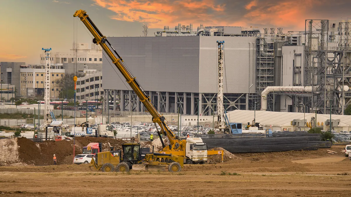
However Fab 38 is nowhere close to able to construct chips but. What I am gazing from throughout the highest of a multi-story automobile park is primarily the foundations of a really costly constructing, wrought from thick girders of metallic and as much as 42 metres into the Earth.
Each sq. metre issues in a fab. Intel avoids having pillars within the fab because of this, and as an alternative makes use of a metallic body circumventing the outer partitions of the constructing. It is not an inexpensive design resolution, neither is it a simple one to hold out. Actually, Intel has employed the world’s second largest crane to elevate the constituent elements of this metallic body into place.
(opens in new tab)
I am instructed Intel had needed the world’s largest crane, however that it was busy constructing a nuclear energy plant within the UK. So it needed to accept the second-largest. Our information tells us that even this crane prices a whole bunch of hundreds of {dollars} to function every day.
The opposite key ingredient for the fab is concrete. The development requires a lot that Intel has three concrete factories arrange devoted to getting it to the location. To get the concrete from these websites to the fab development, a big fleet of vans is required. That causes one other difficulty: congestion. Israel’s primary highways and roads appear in adequate situation, and on our travels it seems to be like they’re constructing much more of them, however we did get caught in site visitors a handful of occasions. To attempt to keep away from inflicting that logistical nightmare, and to not make issues worse for these close by, Intel’s concrete vans solely journey at night time.
The precise date when the fab will probably be completed is not set, but it surely’ll be prepared someday in the midst of the last decade. Possible it’s going to miss out on the primary wave of EUV processes out of Intel, with Intel 4. It takes so lengthy to construct new capability, Intel is basically betting on demand a few years upfront of when it’s going to come. It is a forecasting nightmare: we’re simply off the again of unprecedented demand for silicon and now we’re in a interval of a comparatively gradual marketplace for processors.
But when one other such wave of demand for chips comes once more sooner or later, Intel says it is going to be ready. Fab 38 has extra room to develop if wanted, it is only a matter of when it could possibly rent an especially giant crane.


