Ever questioned what the proper reminiscence chip could be like? Properly, it must be sooner than one of the best DRAM, retailer information for many years at a time so it may very well be used like flash reminiscence, and use much less vitality than each for top effectivity. That may sound like a pipe dream however a workforce of researchers has developed a prototype materials that may very well be the stepping stone wanted to make it a actuality.
This is not a brand new thought, in fact, and we have talked in regards to the progress of ULTRARAM prior to now. That is additionally within the analysis and growth part however it has the potential to succeed in the market, as it really works utterly as supposed proper now. The one downside is that the manufacturing of it must be considerably scaled up, with the fee dropping proper down earlier than it may very well be used as a substitute of DRAM and NAND flash.
Nevertheless, a workforce of scientists at Stanford College has launched a paper within the Nature journal (through Stay Science) that particulars the event of a brand new semiconducting materials that may be stacked right into a superlattice, making it preferrred as the idea of a reminiscence circuit.
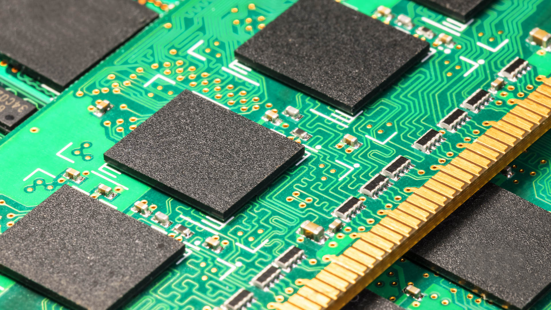
The chips we use for the DRAM in our PCs and VRAM on our graphics playing cards are based on repeated layers of silicon, steel, and insulators. Deep inside them are billions of cells, comprising transistors and capacitors, that quickly retailer cost, which in flip is used to indicate digital data. Whereas very quick, DRAM has a serious downside: The cost naturally dissipates very quickly, so the cells should be periodically refreshed.
On the different finish of the dimensions is NAND flash. It really works in a really roughly related style however makes use of a excessive voltage to entice the cost in an insulated ‘field’, that means it could possibly retain information for very lengthy durations. Higher often called non-volatile reminiscence, flash is utilized in SSDs and USB reminiscence sticks to retailer information for years.
Sadly, it is actually sluggish in comparison with DRAM and the cells put on out over time. What’s wanted is a sort of reminiscence that has all the benefits and not one of the disadvantages, permitting it for use as risky and non-volatile reminiscence. That is the final word purpose of GST467, a mix of antimony, germanium, and terbium the paper’s authors declare can be utilized as the idea of an final, common reminiscence.
So why is that this higher than ULTRARAM? To start with, cells created with the fabric required a far decrease working voltage than its competitor (0.7V versus 2.5V), which fits a good distance in preserving the ability consumption (and subsequently, warmth) underneath management. The paper additionally claims the brand new materials is healthier fitted to implementation with present semiconductor manufacturing applied sciences than related, so-called phase-change supplies.
Nevertheless, the place ULTRARAM is near getting used available in the market already, albeit in sectors that require little or no reminiscence or storage (e.g. Web-of-things, IoT, gadgets), GST467 may be very a lot nonetheless within the lab part of growth. The researchers are hoping to garner curiosity from the reminiscence business to see if their work will be scaled to a degree that it is economically viable to fabricate in giant portions.
For now, although, the quick future is all about ultra-fast DDR5 and GDDR7 for risky reminiscence, with the latter showing later this yr. Samsung, Micron, and others have additionally pumped billions of {dollars} into making large-capacity flash reminiscence chips for one of the best SSDs, in order that they’re unlikely to desert such efforts any time quickly.


